State of The Art - SPARC M8 & Solaris
Abstract:
The SPARC processor was developed by Sun Microsystems and had existed since the exit of major systems manufacturers from the Motorola 68K environment. Multiple manufacturers had always existed in this environment, to provide to consumers multiple supply chains in this commodity hardware market. The migration from 32 bit to 64 bit computing in SPARC occurred decades ago, as current computing systems still wrestle with the complexities. The next increment of hardware from Oracle was released September 17, 2017 - once again maintaining the fastest CPU sockets and SMP systems in the world. It is past 7 months since the release, it is long overdue for an article.
 |
| [SPARC M8 Block diagram, courtesy Oracle T8/M8 Architecture White Paper] |
Block Diagram Layout
A logical
block diagram can help the reader gain a better understanding of the
heart of the system. That author of the Next Platform publication
speculates,
how four S7 processors may have been merged onto the same die or
silicon, using a switched interconnect encapsulated in silicon.
Overall, it does appear to look like a fully switched quad-socket 32 core 256 thread SMP system, burned onto a single piece of silicon. This is a pretty astounding effort, any way one chooses to examine the diagram!
 |
| [SPARC M8 Processor with Oracle & Sun Microsystems SPARC family, Courtesy Oracle] |
Architecture Changes
In general, processors have undergone many changes, mostly regarding consolidation of functions. As time progressed, the pattern of consolidating resulted in lower part counts, higher performance, higher reliability. Components were designed, sometimes combined, sometimes re-separated in various architectures:
- Integer Processing Units
- Floating Point Processing Units
- Memory Management Units
- Processor Socket Cross-Bar Switch
- 1st level cache
- 2nd level cache
- 3rd level cache
- Network Interfaces
- Video Processing
- Encryption Units
- De-encryption Units
- Decompression Units
- [DAX] Database Analytics Acceleration Units
The M8 is no exception... being a server & cloud oriented, video has been de-emphasized for some time & no longer developed actively by Oracle. Previous processors had integrated 10 Gig Ethernet (i.e. Sun Microsystems SPARC T2+) or attempted to integrate Infiniband (i.e. Oracle SPARC "Sonoma" S7) - but Oracle had decided to de-emphasize these commodity features. Oracle, being primarily a software company, concentrated on the most "bang for the buck" with faster cores, encryption, decryption, decompression, and database acceleration units.
 |
| [SPARC Solaris Layered Availability Infrastructure, courtesy Oracle SPARC T8/M8 RAS datasheet] |
Socket Availability Architecture
The SPARC M8 Processor continues to play a vital role in the Availability Architecture of Solaris systems. With the innermost 4 layers of the onion, features like: parity, error correction, reissue on error in hardware, internal power management, voltage scaling, frequency scaling. Decades of design continue to exhibit robust features unavailable in commodity CPU architectures.
 |
| [SPARC Solaris DIMM Sparing Infrastructure, courtesy Oracle SPARC T8/M8 RAS datasheet] |
Memory Availability Architecture
Normally, error correction exists on DIMM's chosen for the SPARC Servers. If one of the DIMM's repeatedly experiences errors on a SPARC M8, Solaris will initiate the process of retiring the faulty DIMM. The hardware can interleave memory across all 16 DIMM's, for maximum throughput, and can also facilitate interleaving memory requests across 15 DIMM's, in order to facilitate a DIMM retirement. During retirement, there is a slight decrease in the amount of available memory.
Virtualization Architecture
The SPARC M8 processor works in combination with
OpenFirmware in order to implement the lowest levels of virtualization.
Physical Domains, which allows for electrically disconnected domains, is facilitated by the LOM (Lights Out Management) card, allowing for an OpenBoot instance to operate on each physical domain (note: this feature is only available on higher end systems.) There are no particular features within Physical Domains, which specifically benefit from the M8 processor.
Within the Physical Domain, a Hypervisor program is run in the OpenFirmware, allowing for virtual instances of OpenBoot to run for different groups of devices (i.e. console, memory, pci-cards slots, network cards, disk devces.) Different OS's may run inside of these logically separated OpenBoot instances. A Logical Domain can be live-migrated to a different Physical domain or even a different SPARC chassis, taking advantage of M8 enbedded engines at wire-speed such as Encryption, Decryption, and Decompression.
Zone virtualization is also available under Solaris, regardless of underlying architecture. The SPARC M8 brings hardware accelerated encryption, decryption, and uncompression for activities like live migration, similar to the benefits to Logical Domains.
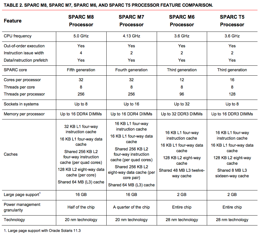
Recent Processor Comparisons
The SPARC M8 processor has certainly advanced in performance over the past few generations of silicon, both from Oracle and Fujitsu. The Register was kind enough to put together a simple chart, illustrating the differences between each of the recent processors, each processor being the fastest socket of it's kind during it's release.
 |
| [Multivendor SPARC Comparison Chart, courtesy The Register] |
Performance Comparisons
As The Register had pointed out, the new core's "wider instruction pipeline... coupled with the increase in clock frequency and the larger L1 code cache" sees to wring out the most recent performance gains from this silicon. These features help to define the 5th generation S5 core, located in the former [1/4 sized] S7 and now M8 processors. Boosting the clock rate nearly 25% from slightly over 4GHz M7 to an industry "unheard of" 5 GHz clearly is beneficial.
 |
| [SPARC M8 Security Features, courtesy Oracle Datasheet] |
Security Comparisons
The Register also
reported important enhancements in security, "it can perform
hardware-accelerated cryptographic functions – such as AES, RSA and
SHA-512 – at twice the speed of the M7." In addition, the SPARC M8 is the only processor in the industry which supports
SHA-3 in silicon. With functions like Random Number Generators and [En|De]Crypto operations in hardware, there are no excuses for lack of security in a data center since there is virtually no cost or processing overhead. Crypto functions operate fast enough to occur at wire-speed for network with virtually unnoticable CPU overhead, reserving the rest of the system resources for processing business/military data.
 |
| [SPARC M8 RDBMS Features, courtesy Oracle Datasheet] |
Database & Analytics Comparisons
The massive thread count with 32x cores, 8x threads per core, 32x floating point units are not unusual for the SPARC M8, although these are already unusually large in comparison to other slower commodity & proprietary processors on the market. These significantly boost application & database performance to non-competitive proprietary Intel and other processors.
The SPARC M8 advances on the former "State of the Art" SPARC M7 with larger caches & faster processing for all workloads, including Database & Analytics.
The real secret of this processor lies in the Next-Generation Data Analytics Accelerator (DAX) engines. In-line decompression enables 200%+ increase in data held in memory for processing without performance impact at 120+ GB/second. Performance improvements of up to 700% for in-memory query acceleration is demonstrated! Oracle number processing is now managed through accelerators,
short-cutting software routines to directly pass processing of numbers
larger than 16 bytes to the hardware for all database workloads,
resulting in 1000% increases in performance! Java 8 Streams API can be used to work with data-sets directly via the DAX, eliminating iteration operations [since they are implied] providing 2000% increase in performance on some operation types!
Conclusion
There are no competing processors in the same Integer or Floating Point Processing Class as the Oracle SPARC M8 processor. Full security, with nearly any cryptography library of choice, is no longer a burden with the SPARC M8... there are no security compromises with this processor, outrunning any workload on any similarly configured socket-to-socket configuration, even with full encryption enabled under SPARC. Once one tries to compare database processing or java application processing, it is quickly observed that many industry players may be a decade or more away in performance of similar workloads. All of this, with the ability to virtualize, with no virtualization performance or monetary tax, makes this an exceptional core to any system in any data center. It will be difficult for any hardware vendor to build any kind of superior next generation processor in the first quarter of the 21st century... the SPARC M8 is the apex of modern day computing.