 [UltraSPARC T3 Micrograph]CoolThreads UltraSPARC and SPARC Processors
Abstract: Processor development takes an immense quantity of time, to architect a high-performance solution, and an uncanny vision of the future, to project market demand and acceptance. In 2005, Sun embarked on a bold path moving toward many cores and many threads per core. Since the purchase of Sun by Oracle, the internal SPARC road map from Sun had clarified.
 [UltraSPARC T1 Micrograph]Generation 1: UltraSPARC T1
A new family of SPARC processors was announced by Sun on 2005 November 14.
- Single die
- Single socket
- 64 bits
- 4, 6, 8 integer cores
- 4, 6, 8 crypto cores
- 4 threads/core
- 1 shared floating point core
- 1.0 GHz - 1.4 GHz clock speed
- 279 million transisters
- 378 mm2
- 90 nm CMOS (TI)
- 1 JBUS port
- 3 Megabyte Level 2 Cache
- 1 Integer ALU per Core
- ??? Memory Controllers
- 6 Stage Integer Pipeline per Core
- No embedded Ethernet into CPU
- Crypto Algorithms: ???
Platform designed as a front-end server for web server applications. With a massive number of cores, it was designed to provide web-tier performance similar to existing quad-socket systems leveraging a single socket.
To understand the ground-breaking advancement in this technology, most processors were single core, with an occasional dual core processor (with cores glued together through a more expensive process referred to as a multi-chip module, driving higher software licensing costs for those platforms.)
 Generation 2: UltraSPARC T2
The next generation of the CoolThreads processor was announced by Sun on 2007 August.
- Single die
- Single Socket
- 64 bits
- 4, 6, 8 integer cores
- 4, 6, 8 crypto cores
- 4, 6, 8 floating point units
- 8 threads/core
- 1.2 GHz - 1.6 GHz clock speed
- 503 million transisters
- 342 mm2
- 65 nm CMOS (TI)
- 1 PCI Express port (1.0 x8)
- 4 Mageabyte Level 2 Cache
- 2 Integer ALU per Core
- 4x Dual Channel FBDIMM DDR2 Controllers
- 8 Stage Integer Pipeline per Core
- 2x 10 GigabitEthernet on-CPU ports
- Crypto Algorithms: DES, Triple DES, AES, RC4, SHA1, SHA256, MD5, RSA-2048, ECC, CRC32
This processor was designed for higher compute intensive requirements and incredibly efficient network capacity. Platform made an excellent front-end server for applications as well as Middleware, with the ability to do 10 Gigabit wire-speed encryption with virtually no CPU overhead.
Competitors started to build Single-Die dual-core CPU's with Quad-Core processors by gluing dual-core processors into a Multi-Chip Module.
 [UltraSPARC T2 Micrograph]Generation 3: UltraSPARC T2+
Sun quickly released the first CoolThreads SMP capable UltraSPARC T2+ in 2008 April.
- Single die
- 1-4 Sockets
- 64 bits
- 4, 6, 8 integer cores
- 4, 6, 8 crypto cores
- 4, 6, 8 floating point units
- 8 threads/core
- 1.2 GHz - 1.6 GHz clock speed
- 503 million transisters
- 342 mm2
- 65 nm CMOS (TI)
- 1 PCI Express port (1.0 x8)
- 4 Megabyte Level 2 Cache
- 2 Integer ALU per Core
- 2x? Dual Channel FBDIMM DDR2 Controllers
- 8? Stage Integer Pipeline per Core
- No embedded Ethernet into CPU
- Crypto Algorithms: DES, Triple DES, AES, RC4, SHA1, SHA256, MD5, RSA-2048, ECC, CRC32
This processor allowed the T processor series to move from the Tier 0 web engines and Middleware to Application tier. Architects started to understand the benefits of this platform entering the Database tier. This was the first Coolthreads processor to scale past 1 and up to 4 sockets.
By this time, competition really started to understand that Sun had properly predicted the future of computing. The drive toward single-die Quad-Core chips have started with Hex-Core Multi-Chip Modules being predicted.
 Generation 4: SPARC T3
The market became nervous with Oracle purchasing Sun. The first Oracle branded CoolThreads SMP capable UltraSPARC T3 was launched in in 2010 September.
- Single die
- 1-4 Sockets
- 64 bits
- 16 integer cores
- 16 crypto cores
- 16 floating point units
- 8 threads/core
- 1.67 GHz clock speed
- ??? million transisters
- 377 mm2
- 40 nm
- 2x PCI Express port (2.0 x8)
- 6 Megabyte Level 2 Cache
- 2 Integer ALU per Core
- 4x DDR3 SDRAM Controllers
- 8? Stage Integer Pipeline per Core
- 2x 10 GigabitEthernet on-CPU ports
- Crypto Algorithms: DES, 3DES, AES, RC4, SHA1, SHA256/384/512, Kasumi, Galois Field, MD5, RSA to 2048 key, ECC, CRC32
This processor was more than what the market was anticipating from Oracle. This processor took all the features of the T2 and T2+ combined them into the new T3 with an increase in overall features. No longer did the market need to choose between multiple sockets or embedded 10 GigE interfaces - this chip has it all plus double the cores.
The market, immediately before this release, the competition was releasing single die hex-core and octal-core CPU's using multi-chip modules, by gluing them together. The T3 was a substantial upgrade over the competition by offering double the cores on a single die.
 Generation 5: SPARC T4
Oracle indicated in December 2010 that they had thousands of these processors in the lab and predicted this processor will be released end of 2011.
After the announcement, a
separate press release indicated processors will have a renovated core, for higher single threaded performance, but the socket will offer half the cores.
Most vendors are projected to have 8 core processors available (through Multi-Chip modules) by the time the T3 is released, but only the T4 should be on a single piece of silicon during this period.
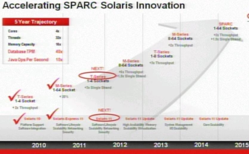 [2010-12 SPARC Solaris Roadmap]Generation 6: SPARC T5
Some details on the T5 were announced with the T4. Processors will use the renovated T4 core, with a 28nm process. This will return to 16 cores per socket again. This processor may be the first Coolthreads T processor able to scale from 1-8 processors. It is projected to appear in early 2013.
Some vendors are projecting to have 12 core processors on the market using Multi-Chip Module technology, but when the T5 is released, this should still be the market leader in 16 cores per socket.
Network Management ConnectionConsolidating most network management stations in a globalized environment works very well with the Coolthreads T-Series processors. Consolidating multiple slower SPARC platforms onto single and double socket T series have worked well over the past half decade.
While most network management polling engines will scale linearly with these highly-threaded processors, there are some operations which are bound to single threads. These type of processes include event correlation, startup time, and syncronization after a discovery in a large managed topology.
The market will welcome the enhanced T4 processor core and the T5 processor, when it is released.


